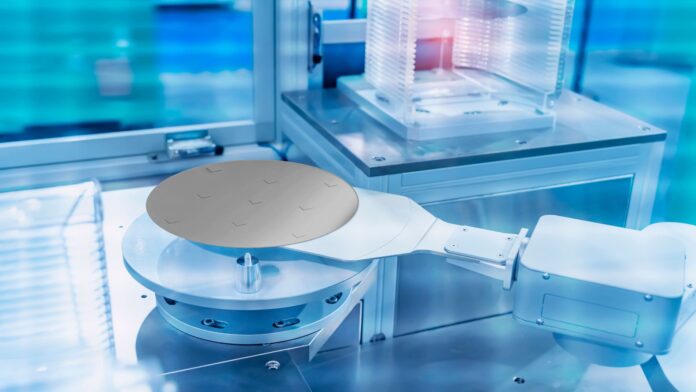
Joensuu, Finland – July 15th, 2024 – Chipmetrics Oy, an innovative metrology solutions provider to the semiconductor industry, announces the launch of two new test chips, the PillarHall LHAR5 and the ASD-1. The PillarHall LHAR5 silicon test chip builds on the success of its predecessor PillarHall LHAR4, with the new LHAR5 test chips being better suited for the most advanced 3D semiconductor device high aspect ratio structures with a gap height as low as 100 nm. Fitting seamlessly into Chipmetrics’ pocket wafer concept, it also allows for fast and accurate process control with full 300-millimeter compatibility.
The PillarHall LHAR5 test chip comes in two variations, with a 100-nanometer and a 500-nanometer gap height. The new 100-nanometer gap height allows engineers to research and compare possible dimensional effects in film penetration depth in line with 500-nanometer gap chips. This allows for new insights into film conformality control and a deeper understanding of 3D NAND, DRAM and other nanoelectronics containing high aspect ratio structures.
“With the launch of PillarHall LHAR5, ASD-1 and the 300-millimeter pocket wafer concept our product line is compatible with the most advanced and challenging semiconductor deposition and etch technologies like ALD, ALE and ASD. The Chipmetrics test chips with our pocket wafer concept is directly compatible with and ready to be used in all existing deposition tools,” says Mikko Utriainen, CEO of Chipmetrics.
The Chipmetrics ASD-1: Prototyping and Process Control for Area Selective Deposition workflows
Launched concurrently with the PillarHall LHAR5 is the Chipmetrics ASD-1 test chip, for prototyping and process control of Area Selective Deposition (ASD) workflows. As the name implies, ASD allows for selective growth of thin films on specific substrate areas, while avoiding it on others, with the ASD-1 test chip aiming to give customers easy access to high-quality data for process control and R&D.
The ASD-1 test chip features a high surface planarity, low line edge roughness, and small line widths which are crucial for ASD applications in advanced semiconductor manufacturing. The ASD-1 test chip features arrays of sub-100 nanometer narrow line structures with alternating materials aligned on the planar silicon substrate for accurately characterizing self-aligned area selective depositions through either Atomic Layer Deposition (ALD) or Chemical Vapor Deposition (CVD) and related processes. The Chipmetrics ASD-1 helps engineers to accelerate ASD process development to meet challenges in miniaturizing and scaling, as well as in reducing defects and improving yield. Both the PillarHall LHAR5 and ASD-1 test chips are available immediately.


